 http://www.wallsave.com/wallpaper/1024x768/circuit-electronics-circuits-505203.html
In this unit there many new concepts that were introduced in order to increase our knowledge on digital circuits and how they work. We learned everything from how computers transport information (binary) along with other base system computer scientists and engineers use, to the making of a digital circuit. In order to make the circuit, it was very important to learn how logic gates and logic probe play a key role in producing different outputs. At the end of the learning process we applied our knowledge to create a a ten LED circuit known as the roulette wheel. We arranged the LED's in different order and made them flash in different patterns using a 555 timer chip and a 4017 IC chip.
 http://www.ee.nmt.edu/~rison/ee308_spr99/lectures.html
The first lesson was on number systems, such as binary, hexadecimal, etc. The computer uses binary number system to transfer data and perform different functions. How ever, binary is not a daily used number system. To better understand this system, people convert them into decimal or in to hexadecimal number systems. The way distinguish these system is by looking at their base digit. For example, the base for binary is two, for decimal is ten, and for hexadecimal is sixteen. These bases act as the multiplier of the system.
 http://www.allaboutcircuits.com/worksheets/gates.html
The next lesson on digital circuit included logic gates. A logic gate can be looked as a circuit that has many out puts (most 2) but only one output. There are a set of 7 gates that are used in many digital circuits to perform different outputs based on the specific inputs. The logic gates can be implement using diodes, transistors and other such devices. The IC chip used in lab two consisted of four NAND gates with two inputs, A and B, and one output, C.
 http://www.engineersgarage.com/tutorials/how-to-measure-calculate-value-of-resistance
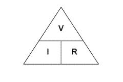
Next we learned about the electronic theory and bread boarding. Voltage is electronic pressure, current is electron flow and resistance is an objects ability to stop current flow. Voltage is current times resistance, current is voltage divided by resistance and resistance is voltage divided by current. These formulas were used when we performed our first lab. We had to calculate the the current passing at different points when the logic probe was in a high or low state. Then the formulas mentioned above were used to find the resistance and the voltage at those points. The information was recorded on a separate chart. The logic probe indicated the binary state of any point on the digital circuit thus the circuit was digital. We also learned the different resistor colors and how to read them in order to figure out the right value of the resistor.
The next lab we performed was performed to see how logic gates worked. The circuit from the previous lab was used during this lab. Different 74LS chips were taken and inserted in to the breadboard and the out put was recorded based on where the logic probe was inserted (what pin). The outputs were recorded and compared to the truth tables of the seven gates. This helped us determine what gates were used in the chip that we were testing.
The third lab we did was to check whether or not the output changed if we had three inputs rather then two inputs. The process was the same as lab two. The only difference was that now there were three inputs. After testing and checking each output, we realized that the results didn't change. So if the first chip with two inputs was discovered to have a AND gate inside, then the same chip with three inputs have the same output thus the AND gate is still there.
http://www.bbc.co.uk/schools/gcsebitesize/design/electronics/calculationsrev1.shtml

The final lab we did for this unit was the roulette wheel. In this lab, we had to make 10 LED s light up in a pattern. To do this a 555 timer chip, 4017 IC chip and resistors were used. The first step in this project was to learn the pin names of the 555 timer and 4017 IC chips as well as their functions. Next we had to replicate the schematic diagram of the roulette wheel that was given to us in a schematic drawing program. After doing this, we were supposed to choose the frequency that the LED s will flash at and calculate the value of the resistor in order to pick the right one. My frequency was 5, so my calculations are:
R2= [(1.44 / (F x C) ) - R1] /2
R2= [(1.44 / (5 x 0.000001F) ) - 1000] /2
R2= [(1.44 / (0.000005) ) - 1000] /2
R2= [(288,000) - (1000) /2
R2= 287,000 /2
R2=143, 500
R2=143,500 K .
After the resistors were collected we began the assembling circuit. The LED s were placed in the bread board first in order to avoid confusion when hooking up the LED s to the 4017 chip. The schematic diagram was closely followed in order to make the circuit the way that will cause the LED s to flash in the order we wanted.
